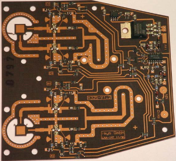
"Franco" SU-02 10GHz PCB
Ex equipment low noise amplifer PCB, featuring PTFE substrate and 4 independent amplifiers (labelled AH, AV, EH and EV) based on the ultra-low-noise pseudomorphic HJ FET NE32584C.
These PCBs have been sourced from RF Microwave shop in Italy (originally run by Franco Rota, I2FHW - hence the nickname of the board) and can be used to make a very good 5.6GHz LNA, 10GHz LNA, 24GHz doubler, or just a source of the NE32584c devices or 50-Ohm microstrip lines.
Original DUBUS article + the NE32584C datasheet: media:Franco PCB.pdf
Circuit diagrams
Published with thanks to Chris, G3WIE for having reverse-engineered the circuits of the Franco board posted the his findings to on the UK Microwave Ops mailing list.
Power supply and biasing
Each Franco board comes with a power supply capable of providing both positive and negative voltage to a single amplifier section at a time, with the input voltage range from approx. 8V (the limiting factor here being the operational range of the first voltage regulator) to about 20V (above which one risks frying the on-board IC). Furthermore, each amplifier section features an active bias section configured to maintain nominal drain current on the NE32584C given the voltages provided by the on-board PSU. For details, see below.
Should you want to use your own PSU and/or use fixed bias instead, keep in mind the following:
- the NE32584C is rated for the absolute maximum drain-to-source voltage of 4.0V and the absolute maximum gate-to-source voltage of -3.0V,
- its nominal drain current is 10mA,
- as usual with a FET, care should be taken keep the magic smoke in by ensuring Vds is present if and only if Vgs is.
On-board PSU
The power-supply section of the board produces the supply voltages of +3.1V and -3.3V for the amplifier sections as well as controlling which of the amps is powered up. The main workhorse here is the hex Schmitt-trigger inverter 74HC14.
To generate supply voltages, energise the "14V" pad near the large voltage regulator. Do not apply more than 20V here, it will damage some of the inverter gates. On the other end of the scale, 8V has been shown to suffice.
Output switching
Switching between AV/EV and AH/EH is achieved by varying the voltage applied to the "14V" pad - anything under approx. 15.5V enables the V pair, anything above that threshold enables the H pair. In the terms of the schematics above, varying the input voltage governs which of the lines labelled A and B is at 0V (which allows the amp connected to it to switch on) and which one is at 5V.
As for switching between AH/AV and EH/EV, which pair receives power is governed by the voltage applied to the pads: "10V" and "RX12". By default, i.e. with both of these pads unconnected, the PSU directs Vdd/Vbb to the E pair. With 12V applied to the "RX12" pad (or 8.5-9V to the "10V" pad), the A pair is powered up instead. In the terms of the schematics above, this affects which of the two bipolar transistors: Q1 and Q2 is switched on.
Active bias
Each of the four amplifier sections features a BJT-based active bias circuit with resistor values chosen so that for the Vdd/Vbb value of 3.1V and the Vgg (bias) voltage of -3.3V, both as provided by the on-board PSU, the NE325 ends up at Vds = 2V and Id = 11mA. The same circuit also serves as an on-off switch - in order for the section in question to operate the "A or B" must be at 0V.
G3WIE has created a spreadsheet which can be used to calculate resistor values for given supply voltages and desired FET parameters, or vice versa: File:Hemt active biasV3.ods
Warning: if you choose to retain the active bias circuit, its is critical for Vdd and Vbb to be tied together as per the original design. If they are not and you suddenly lose Vbb but not Vdd, it's bye-bye FET.
Example of tunable fixed bias
While there are of course many ways of biasing a FET, a common approach is to install a trimmer resistor between the source of Vgg and the FET gate so that bias voltage, and by extension drain current, can be tuned for best signal-to-noise ratio. One way of doing this on a Franco board is as follows:
- Remove Q3 and R19. You might also salvage R15 and R16, as they serve no function with Q3 gone
- Cut the track between R19 was, and R20. Where exactly to do this depends on the amplifier in question; for AV and EH the best place is probably the short length of track between C16 and where the collector of Q3 was, in case of AH and EV aim for the short diagonal track between C16 and C17
- Grab a small trimpot, with maximum resistance of 10k or so. Both PC-pin and SMD should work here so choose whichever you feel more comfortable soldering, that said if you opt for the pins make sure you do not have them short-circuiting other parts of the amp. Install it as follows:
- the first (input) contact - between where R19 was and the cut you have just made
- the second (variable-resistance) contact - between R20 and the cut you have just made
- the third (fixed-resistance) contact - to ground. The pad grounding C17 is quite convenient for this
- IMPORTANT: Before doing anything else, turn the trimpot so that it offers high resistance between R20 and where R19 was. You want to start with low Id
- Connect the wire which will provide Vgg to where R19 was
- Grab a meter and confirm you have got everything wired connectly. You want:
- (high, adjustable resistance + 100R) between the source of Vgg and the drain,
- 10k between the source of Vgg and ground, and
- no short between R20 and ground (if you do measure a short here, before disassembling everything turn the trimpot a little bit away from maximum and try again).
10GHz
With the board in question having been designed for 10GHz operation it is perhaps no surprise that the choice of variants is rather wide here.
Single-stage LNAs by Gerald, F6CXO
Probably the simplest variants (there is one for SMA input and one for direct waveguide input) out there, as bias circuitry and socket fitting aside the only modifications needed is removing a resistor from the RF input line + replacing the resistor on the RF output line with a small DC-blocking capacitor. Claimed performance is 14dB gain, 0.7-0.8dB noise figure. For details see the VHF Communications 3/2004 article on pages 8-10 in the PDF above; the circuit diagram has only been annotated in French but the comments are simple enough to understand for an English speaker).
Two-stage LNA by Pete, GM4BYF
In the aforementioned article Gerald, F6CXO mentions the possibility of combining two Franco amplifier sections into a two-stage device. Indeed, the file above includes (on pages 4-7) an Italian-language article - unfortunately with no translation, and a very low-resolution circuit diagram - featuring photos of two devices which appear to have done just that. However, it has been observed that merely connecting the output of amp one to the input of amp two can cause stability problems.Template:Citation needed
In order to avoid the stability issues Pete, GM4BYF has constructed a two-stage version in which the two amplifier sections are laid out back to back, and connected with a short length of semi-rigid coax fed through a specially drilled hole. Details can be found here: File:Franco 10GHz LNA GM4BYF.pdf.
TODO: add performance data, if/when available
Dual two-stage LNA by Geoff, GI0GDP
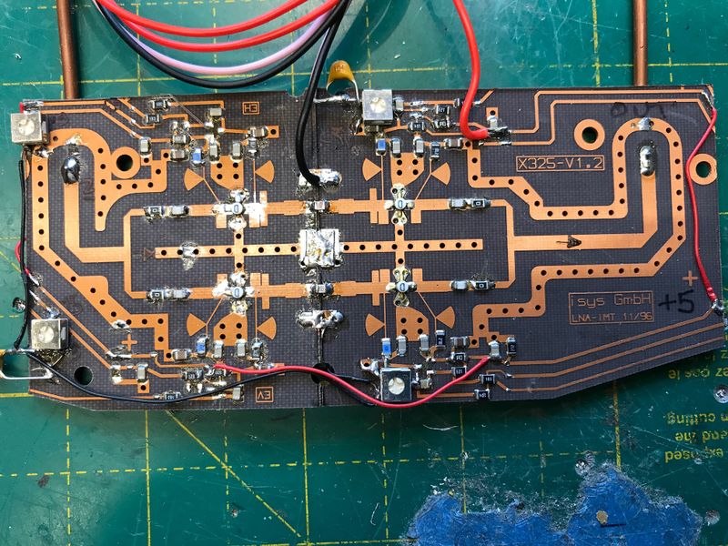
This variant uses two two-stage amplifiers running in parallel to produce around 75mW output from 2.5mW input. In order to avoid excessive amounts of cutting and reassembling the PCB, the two input-stage FETs are turned upside down.
Modification details:
- cut two sections out of a complete Franco PCB: one with both E-pair amps (which will serve as the input stage), one with the A pair (for the output stage)
- join the sections as show in the photo, making sure the back plane is nicely joined (possibly with copper foil + some solder) as well. Make sure the RF lines are not connected, though
- connect the two sections' RF lines using ATC capacitors. Geoff has used 2pF ones here but in his own words, the exact capacitance doesn't really matter
- desolder and turn around the two E-pair FETs
- relocate the E-pair source and drain resistors (yes, all four of them!) to reflect the new orientation of the FETs. When in doubt what goes where, consult the photo
- replace the two 68R drain resistors in the A-pair (i.e. output) amps with jumpers. Note that the photo shows 1R0 rather than 0R chips owing to the fact the author did not have any of the latter at hand at the time
- remove and jumper the four resistors from the RF lines
- make your own biasing arrangements as desired, bearing in mind that with E-pair FETs having been turned around the original active bias circuit will not work without extensive modifications
Nb. Disregard the two through-hole ceramic capacitors, they are only there to provide mechanical support and extra soldering surface.
Two-stage "NE325+MGF1601" LNA by Geoff, GI0GDP
In Geoff's latest take on the subject, a single two-stage assembly has its output-stage NE325 replaced with an MGF1601 clone ("the case is not quite right for a genuine Mitsubishi version but that isn't a show stopper" -- GI0GDP) readily available from Far Eastern suppliers. Reasonably expected performance is 100mW out for 5mW in, that said it will vary depending on the details of your assembly, what kind of enclosure you use (and if it has a lid on or not), and how much time you are willing to spend snowflake-tuning the NE325 gate. Do keep in mind that the two FET types have got quite different voltage and biasing requirements.
The project in question was described in the November/December 2023 issue of Scatterpoint, available to UKuG members.
5.6GHz
The BATC Wiki shows modifications made by Daniel, DL3IAE for the use of a single SU-02 amp in this band.
24GHz
TBA

